
What is PCB Etching? Steps to Ensure an Effective Circuit Board Manufacturing Process
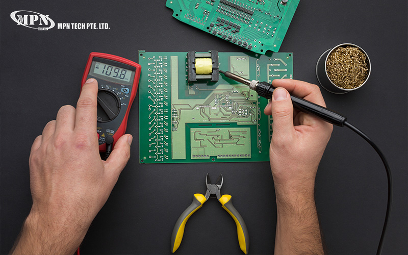
Printed circuit boards (PCBs) form the foundation of almost every modern electronic device, from research prototypes to commercial products. Among the many stages involved in producing a functional board, PCB etching is essential in defining performance, reliability, and manufacturability. This article breaks down the process and highlights the critical steps required to deliver consistent, high-quality outcomes. Keep reading for further insights.
How to Make a PCB Layout
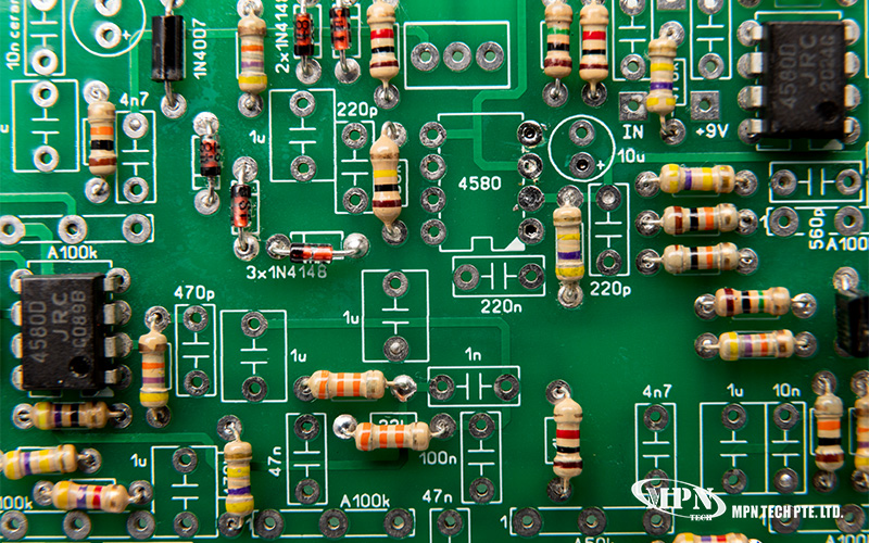
Designing a custom Printed Circuit Board (PCB) is a crucial step in turning a circuit idea into a reliable physical prototype. Understanding how to make a PCB layout correctly allows engineers, researchers, and product developers to move more efficiently from design to testing.
Layout choices directly affect signal integrity, power stability, thermal behaviour, and overall board reliability. Addressing these factors early helps reduce electrical noise and maintain consistent performance across the board. This contributes to a more predictable and efficient transition from schematic design to physical validation. This guide explains the PCB layout process, with a focus on prototyping and research considerations.
 MPN Tech