
Key Takeaways:
How to Make a PCB Layout: A Step-By-Step Guide
- Start with a complete and validated schematic to ensure accuracy throughout the PCB layout process.
- Match schematic symbols to correct footprints to avoid fabrication and assembly issues.
- Group components by function to shorten trace lengths, improve signal integrity, and reduce noise.
- Plan power distribution, routing paths, and grounding early to maintain electrical stability and minimise electromagnetic interference (EMI).
- Consider board size, thermal management, layer structure, and trace sizing to support reliable prototyping and testing.
- Perform thorough design checks and prepare accurate fabrication files to ensure a smooth transition from layout to physical board.
Introduction
Designing a custom Printed Circuit Board (PCB) is a crucial step in turning a circuit idea into a reliable physical prototype. Understanding how to make a PCB layout correctly allows engineers, researchers, and product developers to move more efficiently from design to testing.
Layout choices directly affect signal integrity, power stability, thermal behaviour, and overall board reliability. Addressing these factors early helps reduce electrical noise and maintain consistent performance across the board. This contributes to a more predictable and efficient transition from schematic design to physical validation.
This guide explains the PCB layout process, with a focus on prototyping and research considerations.
How to Make a PCB Layout
1. Begin with a Circuit Diagram
Every PCB layout starts with a complete and validated schematic. Before placing components or routing traces, ensure the circuit diagram reflects the final design intent. PCB design tools such as EasyEDA, KiCad, and Altium allow schematic symbols and electrical connections to link directly to the layout environment. This linkage reduces manual errors and maintains accuracy as the project moves from schematic capture to physical board layout.
2. Link Components to Footprints
Each schematic symbol must be matched to a physical footprint that defines its real-world dimensions, pin spacing, and pad geometry. Incorrect footprints are a common cause of prototype failure. Most design tools include standard libraries. However, for specialised or research-grade components, it is often necessary to create custom footprints based on manufacturer datasheets. Taking time here ensures compatibility during fabrication and assembly.
3. Group Components by Function
Functional grouping is a foundational principle when learning how to make a PCB layout. Divide the board into logical sections such as power regulation, signal processing, and control circuitry. Keeping related components close together shortens trace lengths and reduces resistance along the signal path, preserving signal quality and timing accuracy. Noise-generating or heat-producing components should be positioned away from sensitive analogue or measurement circuits to minimise interference.
4. Select a Power Distribution Strategy
Power routing directly impacts stability and noise levels. A star configuration connects each functional block independently to the power source, helping to reduce voltage drops and noise coupling. A daisy chain configuration, while more compact, may introduce inconsistencies in voltage-sensitive designs. For research prototypes, prioritising electrical stability over space savings is usually the safer choice. As board speed and complexity increase, continuous planes are often preferred over star routing to maintain signal integrity.
5. Route Paths to Reduce EMI
Careful routing is essential to limit electromagnetic interference. Besides keeping traces short and direct, use 45-degree angles rather than sharp 90-degree turns to reduce signal reflections. Abrupt corners can create small impedance discontinuities where signals may partially reflect, especially at higher frequencies. By smoothing the change in direction with 45-degree angles, signal transitions remain more uniform. Routing power and ground traces close together also helps control return paths and lowers EMI.
6. Define the Board Dimensions
Board size and shape should align with the intended enclosure or test setup. Leave adequate clearance around edges for mounting holes, connectors, and probing access. For prototyping, slightly larger boards can make debugging and rework easier without significantly increasing fabrication costs.
7. Address Thermal Considerations
Even prototype boards can experience thermal stress. Identify components that dissipate significant heat, such as voltage regulators or power transistors. Use wider traces, thermal vias, or optional heat sinks to distribute heat effectively. Proper thermal planning improves reliability during extended testing and repeated experiments.
8. Use Dedicated Layer Types
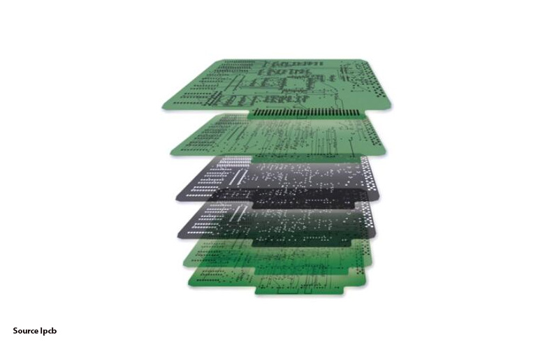
Multi-layer boards are common in modern prototypes. Signal layers handle routing, while power and ground planes provide stable voltage references and reduce noise. A solid ground plane is particularly beneficial for research designs that require accurate measurements or high-speed signals.
9. Connect Layers with Vias
Vias enable connections between layers. Through-hole vias connect all layers and are common in prototypes. Blind and buried vias may be used for more complex designs, but they can increase fabrication costs. Select an appropriate via type to balance performance with manufacturability.
10. Calculate Trace Width and Thickness
Trace dimensions must support the required current without overheating. Online calculators and PCB design tools can help determine safe widths based on copper thickness and current load. This step is essential for avoiding failures during power-up and testing.
11. Apply a Silkscreen Layer
Clear silkscreen markings improve usability during assembly and debugging. Include reference designators, polarity indicators, and orientation markers. For research teams, good labelling saves time and reduces handling errors.
12. Final Checks and File Preparation
Before fabrication, run a full Design Rule Check to identify spacing, clearance, or connectivity issues. Export Gerber files and a complete Bill of Materials. These files are then ready for submission to a fabricator or prototype PCB assembly services, supporting a more reliable transition from layout to physical hardware.
What are Some Common PCB Layout Mistakes?
Even well-designed schematics can underperform if layout fundamentals are overlooked. The following issues are frequently observed in research prototypes and early-stage boards:
- Forgetting return paths increases loop area, leading to noise, crosstalk, and unstable signal behaviour.
- Inadequate decoupling capacitor placement reduces transient suppression, causing power instability during switching.
- Over-tight trace spacing near high voltage raises the risk of arcing, leakage, and insulation failure.
- Incorrect footprint orientation causes assembly errors, polarity issues, and costly rework.
Why a Well-Structured PCB Layout Matters
For teams developing PCB prototypes in Singapore, a well-executed layout plays a part in improving turnaround time and assembly accuracy. Understanding how to make a PCB layout properly enables designers to spend more time validating performance, refining designs, and advancing research.
At MPN Tech, we provide reliable, fast-turnaround PCB fabrication and small-batch PCB prototyping in Singapore, supporting research, development, and early-stage production needs. All of our manufacturing and assembly work follows standardised processes and IPC Class I, II, and III requirements.
Contact us to benefit from our practical engineering insight and performance-focused design support.
 MPN Tech