
Key Takeaways:
What Makes PCBs and PCBAs Essential to Modern Electronics Manufacturing?
- Modern PCB innovations enable high-density layouts that make electronic devices smaller, faster, and more efficient. They are ideal for applications like IoT sensors and biomedical research tools.
- Technologies such as HDI and flexible PCBs improve electrical performance and signal integrity, allowing researchers to produce more accurate, reproducible results in complex systems.Modern PCB innovations enable high-density layouts that make electronic devices smaller, faster, and more efficient. They are ideal for applications like IoT sensors and biomedical research tools.
- Streamlined fabrication methods like SMT and automated assembly reduce time and cost, enabling university teams to rapidly develop and refine low-volume prototypes.
- PCBs and PCBAs form the backbone of multifunctional and intelligent systems across industries, from aerospace and automotive engineering to industrial automation.
Introduction
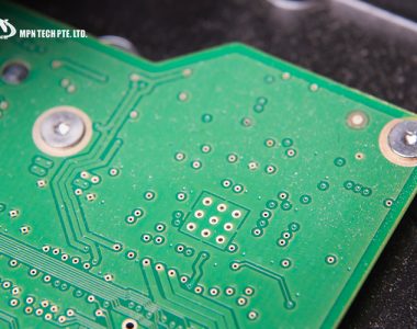
The Printed Circuit Board (PCB) and Printed Circuit Board Assembly (PCBA) form the backbone of electronic innovation. Serving as both the mechanical support and electrical link for components, they make it possible to design devices that are more compact and reliable. From laboratory prototypes to industrial systems, PCBs and PCBAs enable the precise electronic component integration and efficient embedded system design.
This article examines the role of PCBs and PCBAs in advancing electronics manufacturing. Join us as we explore how they continue to shape research, prototyping, and real-world applications.
How Do PCBs and PCBAs Power the Future of Electronics Manufacturing?
1. Miniaturisation and Compact Designs
Innovation in PCB design has allowed electronics to become smaller, faster, and more powerful than ever before. By enabling high-density component placement in compact layouts, PCBs have paved the way for the development of portable technologies, such as IoT sensors and biomedical devices.
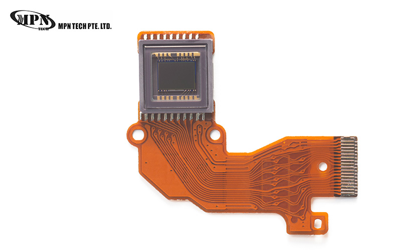
For instance, flexible and rigid-flex PCB layouts support experimental wearables and robotics projects by combining strength, flexibility, and space efficiency. With the help of a reliable PCB supplier in Singapore, researchers can quickly prototype custom designs that balance compactness with functionality.
2. Improved Performance and Reliability
As research applications grow more complex, PCBs must support high-speed data transfer, signal integrity, and mechanical resilience. Advanced technologies such as HDI (High-Density Interconnect) and flexible PCBs enhance the electrical performance and reliability of intricate systems used in 5G, medical diagnostics, and aerospace studies.
In academic research settings, these innovations allow for the development of smaller yet more robust circuits that perform reliably under diverse testing conditions. This helps ensure that PCB fabrication experiments yield dependable and reproducible outcomes, which is critical for ongoing prototyping and system optimisation.
3. Cost Efficiency and Scalability
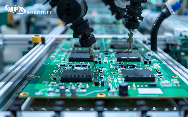
Advancements in PCB and PCBA technology have enhanced both performance and cost efficiency. Using fabrication methods like surface-mount technology (SMT) and automated assembly, manufacturers can shorten production time and reduce material waste. These precision-driven processes optimise component placement and soldering quality, resulting in faster, more consistent builds ideal for research and low-volume production.
Thanks to these efficiencies, university teams and independent labs working on early-stage prototypes can iterate on designs quickly and affordably. With shorter fabrication lead times and reduced costs per board, researchers can produce several prototype versions to evaluate factors like signal integrity, component placement, and thermal performance. This rapid feedback loop ensures more accurate testing and stronger validation of research concepts.
4. Support for Complex Applications
PCBs and PCBAs are fundamental to the design and development of advanced, multifunctional, and intelligent electronic systems used in diverse fields. In industrial automation, aerospace, and automotive engineering, complex multi-layer PCBs manage power distribution, control logic, and sensor data simultaneously.
Within academic research, similar technologies are applied in robotics, environmental monitoring, and communications systems. Local electronic assembly solutions help integrate sensors, microcontrollers, and other components into cohesive, high-performing prototypes. By bridging design and manufacturing, specialists of PCB design in Singapore support both experimental innovation and commercial scalability.
Driving Innovation Through Research and Collaboration
For students, engineers, and professors at Singapore’s leading universities, the ability to design, assemble, and test PCBs rapidly opens new possibilities in innovation and learning. By leveraging electronics manufacturing expertise, academic teams can move from concept to working prototype faster, with reliable results that meet professional standards.
As one of the trusted providers of electronic manufacturing services in Singapore, MPN Tech partners with research institutions and startups to deliver precision, flexibility, and scalability in every project. Developing a single prototype or preparing for pilot production? We are here to ensure your ideas are built on a solid foundation of quality and performance.
Contact us and learn how our electronics manufacturing solutions can advance your innovative ideas.
 MPN Tech