
How to Prepare PCB Files for Fabrication
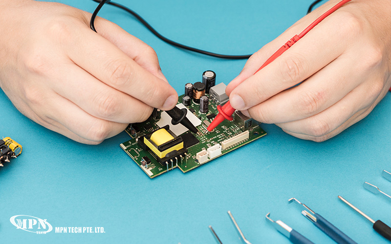
In Singapore’s fast-paced electronics sector, completing a circuit layout marks only the beginning of the manufacturing process. Prior to printed circuit board (PCB) fabrication, or PCB fab, it is important to prepare a complete and technically accurate set of manufacturing files. This documentation package enables a controlled and traceable transition from digital design data to physical board production. This guide outlines the essential files required before submitting your board for fabrication and assembly.
What You Should Know About the Printed Circuit Board HS Code
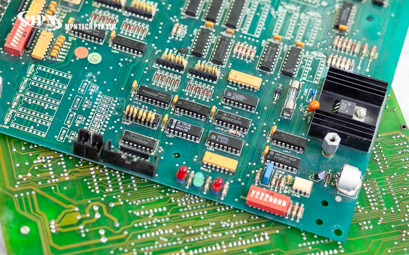
In the electronics industry, efficiency does not stop at design or manufacturing. For companies importing, exporting, or sourcing printed circuit boards (PCBs), regulatory accuracy plays a part in keeping projects on track. One area that is often overlooked until issues arise is the printed circuit board HS code. This code is a standardised international classification used in global trade to identify PCBs for customs purposes.
Understanding how PCBs are classified helps businesses avoid delays, penalties, and unnecessary costs.
What is a PCB Surface Finish and Why is it Important?
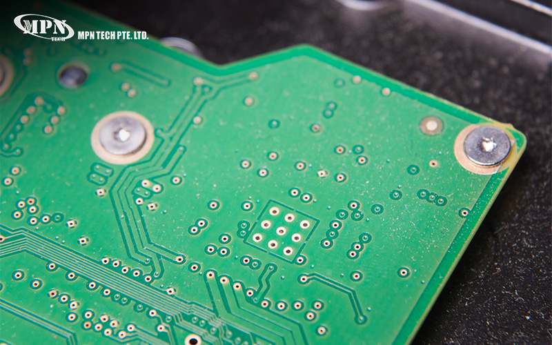
When designing or manufacturing a printed circuit board (PCB), much of the attention understandably goes to layout, components, and electrical performance. However, an often-overlooked decision that plays a critical role in reliability, manufacturability, and long-term performance is the printed circuit board (PCB) surface finish. This protective layer is applied to the exposed copper areas of a PCB. It ensures the board’s pads remain solderable and resistant to environmental damage such as oxidation. If you’re working on PCB prototype projects in Singapore or scaling into PCB assembly, understanding surface finishes is essential.
From Schematic to Gerber: How PCB Design Tools Manage the Full Workflow
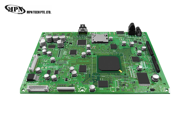
Turning an electronic concept into a manufacturable printed circuit board (PCB) is a process that demands precision at every stage. From defining circuit logic to producing fabrication-ready files, each step must be tightly controlled to avoid errors, delays, and costly rework. This is where modern PCB design tools play a part. This article walks you through the complete PCB design journey, while highlighting common pitfalls to watch out for along the way.
How to Choose the Right PCB Connector
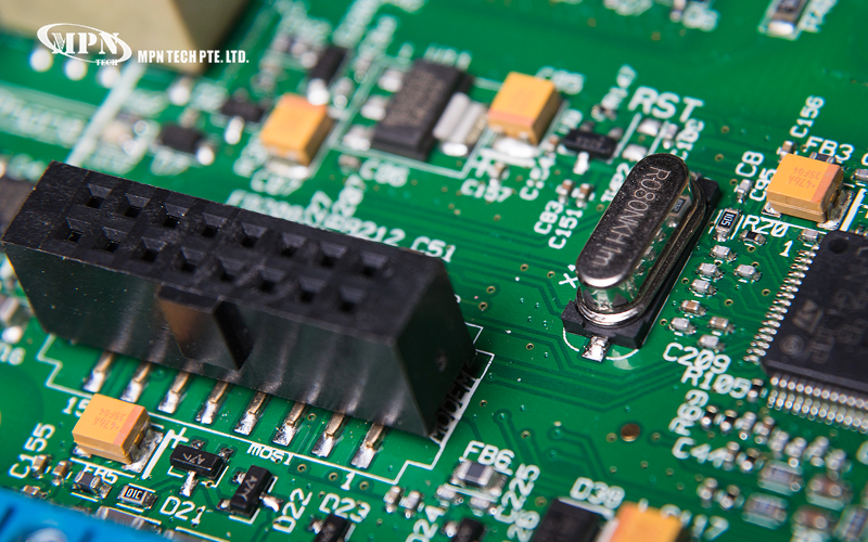
Selecting the right printed circuit board (PCB) connector is a critical step in any electronics project. Connectors act as the interface between a PCB and other components, modules, or external systems. While they may appear to be simple hardware elements, connector choices directly affect electrical reliability, mechanical stability, and long-term performance. This guide outlines the key factors for meeting both functional and physical PCB demands.
Flex PCB vs Ribbon Cable: Which is Better for Compact Designs?
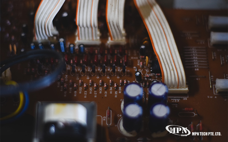
When designing compact electronic systems, the choice of interconnect solution has a direct impact on space efficiency, reliability, and long-term performance. Engineers working on modern devices often compare two common options: flexible printed circuit boards (PCBs) and ribbon cables. Both are widely used to manage internal connections in space-constrained designs, but their strengths differ depending on the application context and operating conditions.
PCB CTE Values Explained: Why Should You Avoid CTE Mismatch?
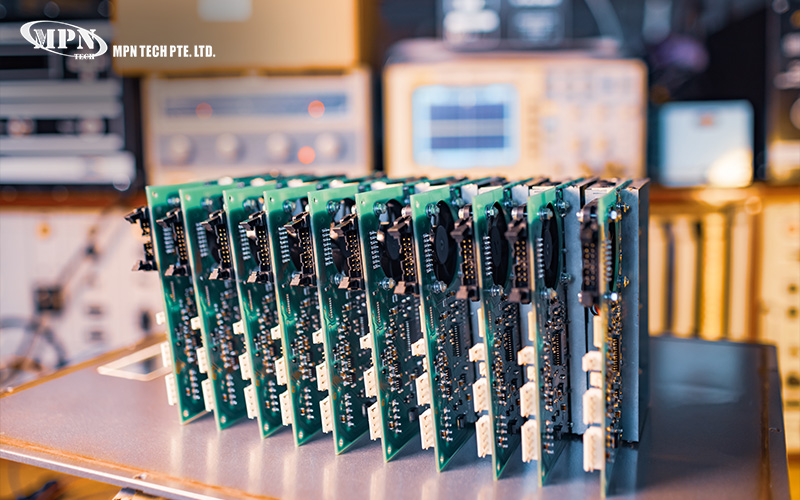
When designing printed circuit boards for prototyping, manufacturing, or research applications, material behaviour under heat is often overlooked. One material property that has a direct impact on long-term reliability is the Coefficient of Thermal Expansion, commonly referred to as CTE. As every material has its own CTE value, differences in expansion behaviour can arise when multiple materials are bonded together within a PCB structure. This article explains what the values mean in practical terms and why managing CTE mismatch is important in reliable PCB design.
RoHS Compliance in PCB Design
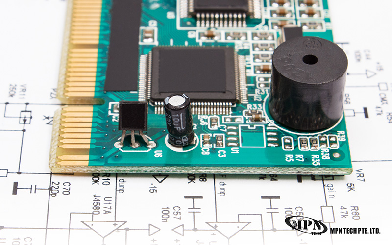
As regulatory requirements, environmental responsibility, and global market expectations continue to evolve, the Restriction of Hazardous Substances (RoHS) compliance has become a fundamental consideration in modern printed circuit board (PCB) design. This article explores the importance of RoHS compliance in PCB design and how it shapes key design and manufacturing decisions.
What is PCB Etching? Steps to Ensure an Effective Circuit Board Manufacturing Process
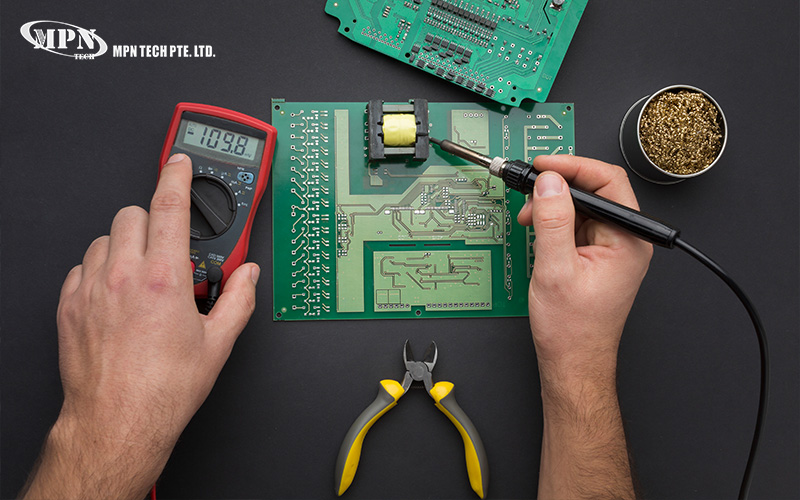
Printed circuit boards (PCBs) form the foundation of almost every modern electronic device, from research prototypes to commercial products. Among the many stages involved in producing a functional board, PCB etching is essential in defining performance, reliability, and manufacturability. This article breaks down the process and highlights the critical steps required to deliver consistent, high-quality outcomes. Keep reading for further insights.
How to Make a PCB Layout
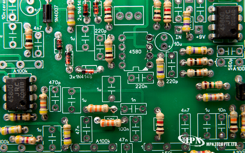
Designing a custom Printed Circuit Board (PCB) is a crucial step in turning a circuit idea into a reliable physical prototype. Understanding how to make a PCB layout correctly allows engineers, researchers, and product developers to move more efficiently from design to testing.
Layout choices directly affect signal integrity, power stability, thermal behaviour, and overall board reliability. Addressing these factors early helps reduce electrical noise and maintain consistent performance across the board. This contributes to a more predictable and efficient transition from schematic design to physical validation. This guide explains the PCB layout process, with a focus on prototyping and research considerations.
 MPN Tech