
Key Takeaways:
What are the Key Differences Between Printed Circuit Board Prototyping and Full Production?
- Prototyping focuses on validating design and functionality, while full production is about manufacturing a finalised PCB reliably at scale.
- Prototyping uses small batches with higher per-unit costs, whereas full production achieves lower costs through high-volume manufacturing.
- Prototyping allows rapid design changes and iteration, while production designs are fixed to maintain consistency and efficiency.
- Prototyping prioritises speed and adaptability, while full production relies on automated, standardised workflows.
- Prototyping emphasises performance and design validation, while production focuses on quality control and consistency across large quantities.
Introduction
In electronics development, the path from an initial idea to a market-ready product involves more than just designing a circuit. Understanding how each stage of the process works is essential for building reliable and manufacturable electronics. Two of the most critical phases here are printed circuit board (PCB) prototyping and full production. While both involve manufacturing PCBs, they address very different needs.
In this article, we examine how prototyping and full production serve distinct purposes. These insights will help teams reduce technical risk and manage costs more effectively throughout the electronics development process.
Printed Circuit Board Prototyping and Full Production: How They Differ
1. Quantity
One of the most visible differences lies in production volume. During prototyping, quantities are intentionally kept low, often between 1 and 10 boards. These small batches allow engineers to validate schematics, layouts, and component choices without committing to large orders.
Full production scales drastically. Once a design is proven, manufacturing moves to hundreds, thousands, or even higher volumes to support market demand or system deployment.
2. Cost Structure
Cost also varies between the two phases. Prototyping typically has a higher per-unit cost. Small batch sizes, specialised handling, and additional engineering checks mean that each board costs more individually. However, this cost is strategic, as it reduces the risk of expensive mistakes later.
In contrast, full production benefits from economies of scale. Automated processes, bulk material sourcing, and streamlined workflows significantly reduce per-unit costs. This is a key consideration when planning PCB manufacturing in Singapore, where efficiency and quality are both expected at scale.
3. Design Flexibility
Design flexibility is another defining factor. Prototyping allows for rapid iteration. In other words, engineers can modify trace layouts, adjust component placement, or refine signal paths based on test results. This flexibility is often a focus in innovative or advanced PCB design projects. It enables quick changes during early development, reducing technical risk before production is finalised.
Once a PCB enters full production, the design is effectively locked. Any changes will require new tooling, revised documentation, and additional validation. All of these factors can increase costs and extend lead times. Conducting thorough prototyping before scaling to production helps minimise these risks later in the process.
4. Manufacturing Process
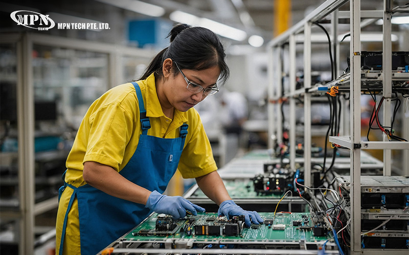
The manufacturing approach also shifts between stages. PCB prototyping often involves more manual processes and shorter lead times. The emphasis is on speed and adaptability rather than throughput. This allows teams to quickly assess whether a design performs as expected.
On the other hand, full production relies on highly automated and optimised manufacturing lines. Processes are standardised to ensure repeatability, yield, and efficiency across large volumes. This structured approach ensures consistency and timeliness.
5. Testing and Validation Focus
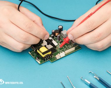
Testing priorities evolve significantly from prototyping to production. When developing a PCB prototype in Singapore, testing emphasises design validation. Engineers examine electrical performance, signal integrity, thermal behaviour, and component placement. The goal is to confirm that the PCB works as intended under real-world conditions.
In full production, testing shifts towards quality control. The focus is on ensuring every board meets specifications, with consistent performance across large batches. Automated inspection, functional testing, and compliance checks become standard practice.
Why These Differences Matter
For researchers and engineers, understanding these distinctions helps bridge the gap between concept and commercialisation. Skipping or rushing PCB prototyping can lead to costly redesigns during production, while overengineering prototypes can slow innovation.
In Singapore’s advanced electronics ecosystem, aligning each phase with its intended purpose ensures smoother transitions. It also improves cost control and outcome quality. By approaching each stage with the right expectations and processes, teams can move confidently from experimentation to reliable, large-scale PCB deployment.
MPN Tech supports PCB projects from research to production through practical engineering expertise and performance-focused layouts. With deep technical expertise in PCB design in Singapore, we help ensure advanced solutions meet international standards and scale efficiently for manufacturing.
Contact us to learn more about our solutions.
 MPN Tech