

Introduction
While a powerful processor is key to modern electronics, the smooth flow of electrical signals is just as important to ensure everything works as it should. No matter how advanced the chipset or how compact the design, if signals become distorted or delayed while travelling through the printed circuit board (PCB), the overall system performance can be compromised.
One crucial factor in this process is signal integrity—how clean and reliable the electrical signals are as they move through the PCB. It plays a part in maintaining the proper functioning of electronic devices.
So, what does signal integrity do, and why is it essential for device reliability? Read on to gain deeper insights.
Key Takeaways:
Why Is Signal Integrity Essential for Modern Electronics?
As signal frequencies rise, PCBs start to behave like transmission lines. Maintaining SI ensures signals stay accurate and reliable, helping to prevent data loss, timing errors, and system failures.
How Can Good Design Prevent Signal Integrity Issues?
SI starts with smart design choices, such as well-planned schematics, controlled impedance, proper layer stackups, and effective capacitor placement, to avoid common issues like EMI, crosstalk, and reflections.
When Should You Identify Signal Integrity Problems?
Early detection is key. Pre-layout simulations, prototype testing, and lab tools like oscilloscopes and TDRs help uncover issues before fabrication or large-scale production, reducing costly revisions.
What Best Practices Improve Signal Reliability?
Ensuring uninterrupted return paths, spacing traces appropriately, and validating designs with both simulation and physical testing help improve performance, reduce errors, and enhance long-term reliability.
Why Does Impedance Matching Matter?
Mismatched impedance causes signal reflections, which distort waveforms and lead to timing errors. Proper trace calculations and layer stackups help maintain consistent impedance throughout the PCB.
What Tools Help Maintain SI?
SI simulations, eye diagram analysis, and lab instruments like time-domain reflectometers (TDRs) are essential for validating designs and identifying issues before mass production.
Understanding Signal Integrity in PCBs
What is it and What Does it Do?
Signal integrity (SI) refers to how well an electrical signal can move through a PCB without being distorted, delayed, or weakened. It is a key aspect of both high-speed digital and analogue circuit design, especially as devices become faster and more compact. The main goal of signal integrity is to preserve signal fidelity. This means ensuring the signal received is as close as possible to the one sent.
In an imaginarily ideal state, an electrical signal would travel from one component to another without any change. But in reality, signal distortion in circuits may happen due to disruptions from various factors, including resistance, interference, or poor PCB layout. While it may not be possible to facilitate perfect transmission, a good SI design should ensure clear and accurate signals throughout their journey on the PCB.
What are the Key Design Practices?
Achieving good signal integrity starts right at the PCB design stage. From schematic planning to routing and component placement, several design choices can make or break signal quality. To maintain strong integrity, keep these key practices in mind:
1. Start with the Schematic and Stackup
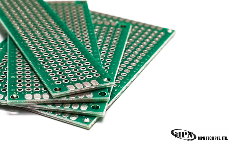
A solid foundation begins with the right PCB stack-up. Carefully assigning layers for power, ground, and signal routing helps with PCB impedance control, signal isolation, and noise reduction. Dedicated ground and power planes provide stable reference points for signals, improving return paths for reduced electromagnetic interference (EMI) and crosstalk between traces.
2. Use Proper Capacitor and Trace Design
Decoupling capacitors matters for power integrity, which directly affects signal performance. Placing capacitors close to power pins helps stabilise voltage and reduce noise. Meanwhile, trace design must account for impedance. It is important to ensure that traces are correctly sized and matched to the system’s needs.
Mismatched impedance can cause signal reflections and loss. Designers must also choose between single-ended or differential pair routing based on the nature of the signal, with differential pairs offering better noise immunity for high-speed signals.
3. Control Interconnect Design
Consider each part of the signal path, starting from the source to the destination. This encompasses traces, pads, vias, and connectors. Compromised interconnects may compromise signals and bandwidths. To maintain signal clarity, each component in the path should be optimised to support the required frequency range and data rate, especially in high-speed PCB designs.
Why Does Signal Integrity Matter?
From smartphones and laptops to advanced automotive and aerospace systems, modern electronics depend heavily on the accurate and high-speed transmission of digital signals. Once signal frequencies exceed roughly 100 MHz, the behaviour of PCBs may shift. Instead of acting as simple electrical connections, they begin to function like complex transmission lines. This change demands a greater focus on signal integrity during the design process.

1. Preserves Signal Quality
Signal integrity ensures that electrical signals maintain their original shape, timing, and voltage levels as they travel through the PCB. This is essential for the correct operation of components that rely on precise timing and data formats.
2. Prevents Transmission Errors
A well-designed PCB with strong SI reduces the risk of signal distortion, noise, or reflections that can corrupt data. This helps avoid communication errors between components and prevents issues like crashes or data loss.
3. Supports High-Speed Performance
As devices operate at higher frequencies and data rates, even minor signal issues may impact the performance. In this case, good SI practices maintain stable, error-free operation in high-speed environments.
4. Ensures Hardware Reliability
Poor signal integrity can cause intermittent faults, erratic behaviour, or even long-term damage to electronic components. By maintaining good SI, designers can enhance the overall reliability and longevity of the hardware.
Addressing Signal Integrity Problems
When Should You Worry About Signal Integrity?
SI becomes even more critical under specific conditions where performance and precision are non-negotiable. As technology advances and devices operate at faster speeds and higher densities, understanding when to prioritise SI can help prevent costly design revisions and product failures.
1. High-Speed Digital Designs
When your system operates at speeds above 1 Gbps, signal degradation becomes a serious concern. At these rates, even small impedance mismatches or layout mistakes can result in reflections, jitter, and data corruption. SI analysis and careful routing become vital to maintain clean, stable signals.
2. RF (Radio Frequency) Systems
RF circuits are highly sensitive to noise and interference. Minor disruptions in signal integrity, such as unexpected coupling or trace discontinuities, can compromise transmission quality and range. This makes proper grounding, shielding, and impedance control crucial.
3. Analogue Systems (Selective Cases)
While analogue circuits are generally less prone to typical digital SI issues, high-frequency or precision analogue systems can still suffer signal degradation. For example, long trace lengths or poorly shielded environments may introduce noise and affect signal accuracy.
4. Any Design Moving Toward High Volume Production
In prototypes, some SI issues may go unnoticed. They often only surface in the mass production stage, showing slight inconsistencies in board materials, trace lengths, or manufacturing tolerances. Addressing SI early keeps the design robust across all units.
What Are Common Signal Integrity Problems to Watch For?
Do not underestimate the importance of design principles. Oversight may trigger SI issues in even the most well-designed circuits. Here are some common problems engineers need to watch out for when designing high-speed PCBs:
1. Electromagnetic Interference (EMI)
High-speed signals can unintentionally radiate energy, especially from poorly routed traces or via stubs. This radiation may interfere with nearby components or systems. EMI often stems from bad layout practices or blocked return paths that force current to flow in noisy, unpredictable ways.
2. Crosstalk Between Traces
When two or more signal traces are routed too closely, electrical signals from one can “leak” into another. One common mishap is placing them side-by-side. This unwanted coupling, known as crosstalk, introduces noise that can distort signals and create unpredictable behaviour.
3. Simultaneous Switching Noise (SSN) / Ground Bounce
In digital circuits, when multiple outputs switch at the same time, they can create a temporary voltage shift in the ground plane. This phenomenon, known as SSN or ground bounce, may result in false triggering and erratic circuit behaviour due to unstable reference voltages.
4. Impedance Mismatch and Reflections
Traces that don’t maintain consistent impedance cause part of the signal to reflect toward the source. These reflections distort the signal’s shape and timing, leading to data errors. This highlights the importance of controlled impedance design in high-speed layouts.
5. Signal Attenuation Over Long Traces
As signals travel over long PCB traces, especially at high frequencies, they begin to weaken due to resistance and dielectric losses. This results in reduced voltage levels and timing delays, which can make signals harder to detect or misinterpreted at the receiving end.
How to Identify Signal Integrity Issues
Catching SI problems early in the design cycle is key to avoiding costly delays and rework during prototyping or production. Follow these methods to detect irregularities before they escalate to major issues:
1. Simulation Tools
Pre-layout and post-layout SI simulations allow designers to model how signals behave across traces, vias, and components. These SI simulation tools help identify reflection, crosstalk, or timing problems before electronic PCB assembly or manufacturing.
2. Prototype Test Boards
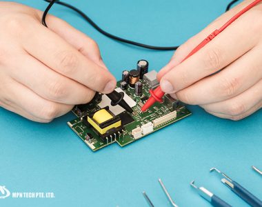
Building prototype boards lets you evaluate SI in real-world conditions. Using test points and controlled layouts, engineers can validate simulation results and identify issues that may not have been predicted.
3. Lab-Based Signal Integrity Testing
Advanced measurement tools like oscilloscopes, time-domain reflectometers (TDRs), and eye diagram analysis can be used to inspect signal quality on a physical board. Such signal quality testing techniques provide a visual and quantitative view of signal degradation, jitter, and impedance mismatches.
What Are the Best Practices to Follow?
In this section, we will share some of the best practices to ensure the production of higher-performing electronic systems. Complementing these with simulation techniques and hands-on testing may help to prevent SI issues.
1. Control Impedance
For high-speed signals, maintaining consistent impedance along the trace is crucial. This involves calculating trace width, spacing, and selecting an appropriate layer stackup to match the signal’s expected characteristics.
2. Provide Uninterrupted Return Paths
Always route high-speed signals over a continuous reference plane (typically ground or power). A clear return path minimises loop area, reduces EMI, and preserves SI by preventing signal distortion due to unpredictable current flow.
3. Minimise Crosstalk and EMI
To limit unwanted coupling and noise, keep enough spacing between signal traces. Pay close attention to those running in parallel. Where possible, use orthogonal routing on adjacent layers (e.g., horizontal on one, vertical on the next) and incorporate ground shielding for added isolation.
4. Validate with Simulation and Testing
Even the best design assumptions need verification. Besides running SI simulations throughout the design process, it is equally essential to use lab tools like TDRs and eye diagrams to confirm the good functionality of PCBs.
Frequently Asked Questions
1. What are some signs of signal integrity issues?
- Glitches or noise in signal waveforms
- Data transmission errors
- Unexpected behaviour in digital circuits
- Failed compliance tests for protocols like USB, DDR, PCIe
2. What’s the difference between signal integrity and power integrity?
Signal integrity focuses on maintaining clean, undistorted signal transmission across PCB traces. Power integrity ensures stable voltage levels and clean power delivery to components.
3. Can poor layout override good component selection?
Absolutely. Even high-quality components can underperform if the layout introduces noise, mismatches, or poor routing. Good signal integrity is as much about layout as it is about parts.
Conclusion
Recognising and addressing SI challenges early in the design phase is key to building reliable, high-speed systems that perform as expected. Poor SI can lead to costly failures, data corruption, and inconsistent performance, especially as PCBs start to behave more like transmission lines at higher frequencies.
Looking ahead, SI will play an even greater role as trends like 5G, artificial intelligence, and edge computing drive demand for faster, more compact PCBs. Designers must be equipped to manage complex routing, tighter tolerances, and more aggressive signal bandwidths.
At MPN Tech, we understand the stakes. As one of the leading PCB design companies in Singapore, we combine technical expertise with unmatched speed and flexibility to meet your needs. Ready to stay ahead of the curve? Let us assist you with same-day service, custom-tailored solutions, and cutting-edge R&D support.
Contact us for a service quote.
 MPN Tech