

Key Takeaways:
PCB manufacturing tolerances define the acceptable variation in PCB dimensions and features, including trace width, hole size, and layer alignment.
Small variations can affect electrical performance, mechanical fit, component placement, soldering quality, and long-term product reliability.
Fine-pitch components, BGA, QFN, multi-layer boards, and high-density layouts generally require closer attention to tolerance planning.
Introduction
In Printed Circuit Board (PCB) manufacturing, tolerances define the acceptable limits of variation in dimensions such as trace width, hole size, board thickness, solder mask alignment, and layer registration.
Although these variations are often very small, they can affect electrical performance, component fit, soldering quality, mechanical assembly, and long-term reliability. Their impact becomes more significant in boards that use fine-pitch components, Ball Grid Array (BGA), Quad Flat No-Lead (QFN), multi-layer structures, or high-density routing, as these designs allow less room for dimensional variation.
Considering PCB manufacturing tolerances early helps reduce drilling, alignment, component fit, and assembly issues while supporting more consistent board performance.
What Are PCB Manufacturing Tolerances?
PCB manufacturing tolerances define the permitted range of variation that can occur during fabrication. Even with controlled processes, small differences can arise in drilling, routing, copper deposition, etching, lamination, solder mask application, and other production stages.
These variations matter because a PCB must do more than match its intended dimensions. It also needs to support reliable electrical connections, accurate component placement, mechanical fit, and repeatable assembly. For example, a narrower trace may increase resistance, while a misaligned drill hole or solder mask opening can affect component fit and soldering quality.
For this reason, tolerances are a key part of PCB quality control and long-term product reliability. Clear, realistic limits help ensure boards can be produced consistently without compromising critical features, especially in products exposed to heat, vibration, thermal cycling, or sustained electrical loads.
Key PCB Tolerances That Affect Reliability
Different PCB features respond to dimensional variation in different ways. Understanding which areas are most sensitive helps design teams decide where tighter control is justified.
Trace Width and Spacing Tolerances
Trace width affects current capacity, resistance, and, in some designs, impedance. If a trace is narrower than intended, it may carry less current or generate more heat. Spacing variations can also increase the risk of shorts, crosstalk, or signal issues, especially in dense or high-speed PCB design projects.
Drill Hole and Via Tolerances
Drill holes must be accurate enough to support component leads, mounting points, and plated connections. Holes that are too small or large can affect fit and connection quality. In multi-layer boards, via tolerances also influence plating consistency and electrical continuity.
Board Thickness Tolerances
Board thickness affects rigidity, enclosure fit, connector compatibility, and controlled impedance. Even small variations can cause issues in products using card-edge connectors or tightly fitted housings, so consider thickness alongside stack-up and material selection.
Copper Thickness Tolerances
Copper thickness affects current capacity, resistance, heat handling, and trace formation. An unsuitable copper thickness tolerance can influence electrical performance, particularly in high-current circuits, and may also affect the final dimensions of fine traces.
Solder Mask Registration Tolerances
Solder mask registration refers to how accurately the mask aligns with pads and exposed copper. Excessive misalignment can partially cover pads or expose unintended areas, increasing the risk of soldering defects, especially with fine-pitch components.
Layer Registration Tolerances
Multi-layer PCBs rely on accurate alignment between internal and external copper layers. Misregistration can affect vias, pads, internal routing, and controlled impedance structures. In highly dense boards, the available clearance between drills and internal copper may be small, so layer alignment becomes increasingly important.
How Tolerances Affect PCB Assembly
Fabrication tolerances directly affect how smoothly a PCB moves into assembly. Even if the bare board meets fabrication requirements, variations in pad geometry, hole size, solder mask openings, or board dimensions can still create problems during component placement and soldering.
For example, incorrect hole sizing can make through-hole insertion more difficult, while dimensional changes around surface-mount pads can affect solder joint formation. These risks become more significant in dense layouts and with BGA or QFN packages, as their smaller connection points leave less room for variation.
For this reason, businesses evaluating a PCB printing service should consider fabrication and assembly together. The goal is to produce a compliant board that can also be assembled consistently.
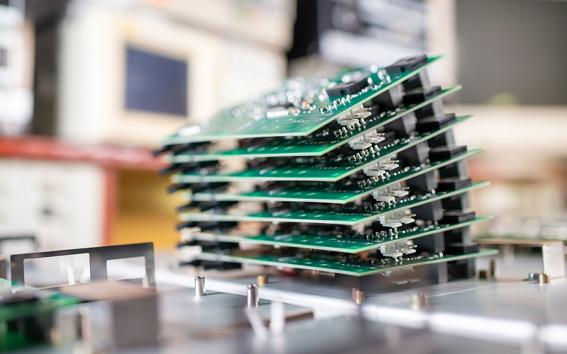
How to Plan for Better PCB Tolerance Control
Better tolerance control begins before fabrication. Businesses need to identify which dimensions affect performance, assembly, and product fit, and which can fall within standard manufacturing limits. Clear planning helps reduce fabrication issues, assembly delays, and unnecessary rework.
Identify Critical Dimensions Early
Not every PCB feature requires the tightest possible tolerance. Design teams should identify features that directly affect electrical performance, mechanical fit, or assembly. These can include controlled impedance traces, connector positions, mounting holes, high-current paths, BGA escape routing, and fine-pitch footprints. Focusing on genuinely critical dimensions avoids imposing unnecessarily tight specifications across the whole board.
Match Design Requirements With Manufacturing Limits
A design should match what the fabrication process can achieve consistently. Overly tight limits can increase cost and complexity, while tolerances that are too loose may affect sensitive features. Therefore, it is important to align manufacturing tolerances with actual production capabilities.
Document Tolerances Clearly
Critical tolerance requirements should be documented clearly in fabrication drawings, stack-up information, and production notes. This helps suppliers identify which dimensions need tighter control and which can follow standard process limits.
Review Fine-Pitch and High-Density Areas
BGA, QFN, and other fine-pitch packages leave limited space for dimensional variation. Businesses should review pad geometry, solder mask clearances, via positioning, routing density, and assembly access together. Doing so helps identify whether certain areas require additional process control before boards enter production.
Work With an Experienced PCB Supplier
Reliable PCB production depends on controlling the tolerances that affect electrical performance, component fit, soldering, and assembly. Working with an experienced supplier early can help identify potential manufacturability issues before they lead to rework or production delays.
MPN Tech Assembly supports customers through Singapore-based operations, allowing closer review of design, fabrication, and assembly requirements throughout the production process. Our PCB assembly capabilities also make it easier to address tolerance-related issues, clarify technical requirements, and move from prototype evaluation to production without unnecessary coordination delays.
With no minimum order quantity, we can support projects from single prototypes to larger production runs. Our engineering team also provides practical support for R&D, New Product Introduction (NPI), and production optimisation, including projects involving fine-pitch components, BGA, QFN, high-density layouts, and tighter PCB manufacturing tolerances.
If your project requires reliable fabrication and assembly support, contact us to discuss your PCB requirements.

 MPN Tech