
Key Takeaways:
What is the Role of PCB Design Tools in the PCB Design Workflow?
- These tools support the entire workflow by maintaining consistency from schematic creation through to Gerber export.
- They help translate early design decisions accurately into layout, enforce electrical and manufacturing rules, and identify potential issues through automated checks and 3D visualisation.
- By integrating BOM generation and manufacturing outputs within a single environment, these tools enable smoother coordination with suppliers and a more reliable transition from design to production.
Introduction
Turning an electronic concept into a manufacturable printed circuit board (PCB) is a process that demands precision at every stage. From defining circuit logic to producing fabrication-ready files, each step must be tightly controlled to avoid errors, delays, and costly rework. This is where modern PCB design tools play a part. By guiding engineers from schematic capture through layout, validation, and Gerber generation, these tools help ensure that designs are electrically sound and aligned with production requirements.
This article walks you through the complete PCB design journey, while highlighting common pitfalls to watch out for along the way.
Why the End-to-End Workflow Matters
PCB design is not just about routing traces on a board. It is a structured process where early decisions directly affect manufacturability, cost, and reliability. The right PCB design tools integrate schematic design, layout, validation, and documentation into a single environment, allowing engineers to detect issues early. For teams working with PCB design companies in Singapore, a clean and well-managed workflow ensures smoother collaboration and fewer production surprises.
What Does the Full PCB Design Workflow Involve and How Do PCB Design Tools Support It?
1. Schematic Capture
The workflow begins with schematic capture. Schematic capture involves creating a logical representation of the electronic circuit. It is done by using standard symbols to represent components and lines to represent electrical connections.
Using the right design tools, engineers select components from built-in libraries or custom libraries and assemble them into a complete circuit diagram. This stage establishes critical details, such as pin connections, signal names, voltage levels, and functional relationships between components.
2. Footprint Assignment
Once the schematic is complete, each component must be linked to a physical footprint. In this stage, engineers select or create footprints that match the exact package type, dimensions, and pin layout specified by the component manufacturer.
It is essential to consider factors such as pad size, pitch, orientation, and assembly method. Design tools help manage this process by associating schematic symbols with verified footprint libraries, maintaining consistency between the circuit design and the PCB layout.
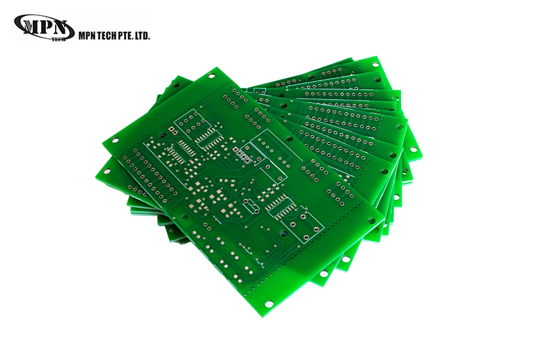
3. PCB Layout
In the layout phase, components are arranged on the board, whereas copper traces are routed to connect them. Placement decisions influence not only whether the board can be manufactured, but also how well it performs electrically and thermally in real operating conditions. At this stage, considerations such as signal integrity, impedance control, electromagnetic interference, and heat dissipation become increasingly important.
Poor routing choices can introduce noise, signal degradation, or thermal hotspots that compromise reliability. Modern design tools support this process by providing routing constraints, visual feedback, and analysis features that help engineers balance performance, manufacturability, and space limitations throughout the process.
4. Design Rule Checks (DRC/ERC)
After placement and routing are completed, the design must be systematically validated to ensure it meets both electrical and manufacturing requirements. This is the stage where Electrical Rule Checks (ERC) and Design Rule Checks (DRC) come into play. ERC focuses on the logical correctness of the circuit. DRC, on the other hand, evaluates the physical layout against predefined manufacturing rules.
Design tools automate these checks by continuously evaluating design data against predefined electrical and manufacturing rules. Connections, component definitions, trace dimensions, and clearances are assessed in the background, with any violations flagged either in real time or through structured reports. Visual indicators, consolidated error lists, and guided highlights help engineers quickly identify and interpret issues that may be missed during manual inspection.
5. 3D Preview
3D visualisation allows engineers to inspect the assembled board before it is built. The process involves generating a three-dimensional representation of the final PCB within the design environment. Using layout data alongside component height and mechanical information, designers can view the board as it would appear once fully assembled.
This capability makes it easier to evaluate physical fit, component orientation, and spatial relationships early in the design process. It is important for compact and enclosure-driven products, where board size, connector placement, and height clearances are tightly constrained.
6. BOM Generation
A Bill of Materials (BOM) is generated directly from the design database, providing a structured list of all components required for production. It typically includes part numbers, descriptions, quantities, package types, and reference designators, ensuring alignment between the design, sourcing, and assembly stages.
As the BOM is linked to the schematic and layout, the design’s updates are automatically reflected. This helps reduce the risk of inconsistencies and allows teams to coordinate more effectively with suppliers and manufacturers.
7. Gerber Export
The final step in the PCB design workflow is exporting Gerber files and drill data for fabrication and assembly. Gerber files are the industry-standard format used by manufacturers to interpret the physical construction of the board. They define each copper layer, solder mask, silkscreen, solder paste, and the overall board outline, while drill files specify hole sizes and locations for vias and component leads.
At this stage, design tools compile all verified layout data into a complete manufacturing package. Engineers typically review layer assignments, polarity, and file completeness to ensure nothing is missing or incorrectly generated.
What are the Common Considerations and Pitfalls to Watch For?
Even with advanced design tools, careful attention is required throughout the workflow to avoid issues that can surface late in the process.
- Using incorrect or unverified footprints can result in components that do not fit the board or cannot be assembled properly.
- Failing to align trace widths, clearances, and stack-up choices with manufacturer capabilities can cause fabrication rejection or redesigns.
- Relying on final-stage checks instead of running DRC and ERC throughout the design increases the risk of hidden electrical or layout errors.
- Overlooking mechanical constraints, such as enclosure fit or connector height, can lead to boards that physically cannot be integrated into the final product.
- Exporting Gerber files without a thorough review can result in missing layers, incorrect polarity, or incomplete drill data, delaying production.
Most of these issues can be avoided through a disciplined, end-to-end design approach. Maintaining accurate libraries, validating decisions at each stage of the workflow, and reviewing outputs before handoff all help reduce risk. When schematic design, layout, verification, and manufacturing preparation are treated as a connected process, PCB design projects in Singapore can move more smoothly from concept to production.
Bringing It All Together
From schematic to Gerber, modern PCB design tools provide a structured framework that supports accuracy, collaboration, and manufacturability. For teams working on projects, mastering this workflow helps bridge the gap between design intent and reliable production.
By working with a trusted PCB supplier in Singapore, like MPN Tech, a disciplined, tool-driven workflow can be established from the outset. With support for both manual and automated assembly processes, hybrid assembly for precision electronics, and IPC Class I, II, and III builds, manufacturing considerations are integrated early in the development cycle. Our expertise helps ensure smoother transitions from design to production, with fewer revisions and more predictable outcomes.
Contact us to learn how our solutions can support your electronics projects.
 MPN Tech