
Key Takeaways:
What Factors Should Be Considered When Selecting a PCB Connector?
- The connector’s current rating should comfortably exceed expected operating and peak loads to minimise the risk of overheating and long-term degradation.
- Pin pitch is another key consideration, as it directly affects layout feasibility and manufacturing precision, with tighter spacing enabling high-density designs and wider spacing offering greater tolerance during assembly.
- Mounting type should be chosen based on the board’s stress conditions and assembly process.
- Finally, mating cycle requirements should reflect how the connector will be used in practice, ensuring durability aligns with servicing and handling needs.
Introduction
Selecting the right printed circuit board (PCB) connector is a critical step in any electronics project. Connectors act as the interface between a PCB and other components, modules, or external systems. While they may appear to be simple hardware elements, connector choices directly affect electrical reliability, mechanical stability, and long-term performance.
Poor connector selection can result in signal degradation, overheating, intermittent connections, or physical strain on the board. For engineers, designers, and developers working on projects in the electronics ecosystem, understanding how to evaluate connectors properly is an essential part of the design process.
This guide outlines the key factors for meeting both functional and physical PCB demands.
Why PCB Connector Selection Matters
Connectors are not just a point of contact. They determine how power, data, or signals move between the board and the rest of the system. When connectors are mismatched to current levels, mechanical stresses, or spatial constraints, they often become the weakest link in the assembly.
In professional PCB design projects in Singapore, connector decisions are often made early, as they influence routing, board layout, and enclosure design. A connector that is too bulky may restrict trace placement. Meanwhile, one with insufficient current capacity may introduce thermal risks. Reliable designs account for these factors before layout begins, reducing costly revisions later.
What to Consider When Choosing a PCB Connector
Understanding application requirements is the first step. The following factors provide a structured way to evaluate connector options.
1. Current Rating
Current rating defines how much electrical current a connector can safely carry. Choosing a connector that operates too close to its maximum rating increases the risk of overheating, voltage drop, or long-term material degradation.
Designers should calculate the maximum expected current under real operating conditions, including peak loads, and select a connector with sufficient margin. This is important in power delivery circuits or applications with sustained current flow.
2. Pin Pitch
Pin pitch refers to the spacing between connector pins. As boards become smaller and more complex, pin pitch plays a major role in layout feasibility and signal integrity.
Tighter pin spacing supports high-density designs but requires more precise manufacturing and soldering. Wider pin pitch offers greater tolerance and mechanical robustness, which can benefit industrial or lower-density applications. The optimal choice depends on board size, signal requirements, and manufacturing capabilities.
3. Mounting Type
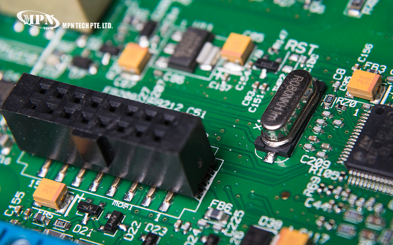
Connectors are typically available as through-hole or surface-mount types. Through-hole connectors provide strong mechanical anchoring, making them suitable for connectors that experience frequent plugging or mechanical stress.
Surface-mount connectors take up less vertical space and support compact layouts, but they rely more heavily on solder joint integrity. The mounting type should align with the board’s mechanical demands and the overall assembly process.
4. Space Constraints
Physical space is a constant limitation in modern electronics. Connector height, orientation, and footprint must fit within both the PCB layout and the final enclosure. Overlooking these constraints can lead to routing difficulties or mechanical interference during assembly.
Low-profile connectors help reduce overall product thickness, while right-angle connectors can redirect cable paths to save space or improve cable management. Designers should review enclosure drawings and mechanical clearances early to avoid conflicts later in the project.
5. Mating Cycles
Mating cycles indicate how many connect and disconnect operations a connector can withstand before performance is affected. Connectors with high mating cycle ratings are well-suited for applications that involve frequent servicing or testing.
For fixed installations where connections are rarely changed, standard connectors may be sufficient. This is because they are not exposed to repeated mechanical stress. In such cases, matching connector durability to real operating conditions helps prevent premature failure. At the same time, it keeps the design efficient and fit for purpose.
How to Align PCB Connector Choices With Manufacturing Realities
The selection process should not take place in isolation. While electrical specifications and mechanical requirements are essential, practical manufacturing considerations play an equally important role in determining whether a design can be produced reliably and efficiently. Factors such as soldering methods, inspection access, assembly tolerances, and component availability all influence final production outcomes.
In the electronics industry, close collaboration between design teams and PCB assembly companies in Singapore helps bridge the gap between schematic decisions and real-world production. Early alignment allows potential assembly challenges, such as fine-pitch soldering constraints or clearance issues, to be identified before fabrication begins.
At MPN Tech, we review connector choices within the broader context of fabrication and assembly requirements. By supporting both manual and machine assembly processes, hybrid assembly for precision electronics, and IPC Standard Class I, II, and III builds, manufacturing considerations are incorporated early in the development cycle.
Contact us to learn how manufacturing-aligned design support can streamline your PCB projects.
 MPN Tech