
Key Takeaways:
What are Some Typical PCB Issues and How They Occur?
- Signal integrity issues occur in high-speed or sensitive designs when signals cannot travel cleanly across the PCB. They often lead to data errors or unstable circuit behaviour.
- Soldering problems are common in low-volume, manually assembled boards. They can result in unreliable electrical connections or complete circuit failure over time.
- Thermal management issues are frequently overlooked in early prototypes, but may surface during testing. They often affect component reliability and performance stability.
- Component placement errors often arise in early-stage or frequently revised designs, potentially causing assembly issues or non-functional components once powered.
- Electromagnetic interference (EMI) can disrupt circuit performance and measurement accuracy. It introduces noise into sensitive signal paths, leading to unpredictable behaviour during testing.
Introduction
Printed Circuit Boards (PCBs) form the foundation of most electronic systems, providing the structure and connections that allow components to work together. From early-stage research prototypes to complex experimental hardware, PCBs play a part in determining how reliably a design performs and how efficiently it can be refined during development.
In academic and Research & Development (R&D) settings, PCBs are often produced in very small quantities for testing, validation, or proof-of-concept work. At this scale, even minor design or manufacturing issues may lead to delays, repeated revisions, or the need for rework.
Therefore, it is essential to understand common PCB issues and how they arise. Early identification of potential design or manufacturing challenges helps minimise rework and streamline troubleshooting. Keep on reading for further insights.
What are Some Common PCB Issues and How to Avoid Them?
1. Signal Integrity Issues
Signal integrity issues are a common PCB problem in high-speed or sensitive electronic designs. They occur when electrical signals are unable to travel cleanly from one point to another on a PCB.
In high-speed or sensitive designs, signals switch rapidly and behave more like waves than simple on-off currents. When traces are poorly routed, too long, or lack proper grounding and impedance control, parts of the signal can reflect, weaken, or interfere with nearby signals. These disturbances tend to alter the shape or timing of the signal, which may cause data errors or compromise circuit behaviour.
How to avoid it:
- Keep critical signal traces as short and direct as possible
- Use proper grounding techniques, including solid ground planes
- Maintain consistent trace widths and controlled impedance where required
- Separate high-speed signals from noisy power or switching circuits
2. Soldering Problems
Soldering defects are another frequent source of PCB pitfalls, especially in low-volume builds that rely on manual assembly. These problems arise when solder does not form a proper electrical and mechanical connection between components and pads.
Uneven heating, insufficient solder, or inaccurate component placement may result in cold solder joints, solder bridges, or misaligned parts. Over time, these defects can escalate to intermittent connections, increased electrical resistance, or complete circuit failure.
How to avoid it:
- Use clearly defined footprints and correct pad sizes in the design stage
- Follow consistent soldering profiles, even for small batch assembly
- Inspect joints visually and, where possible, electrically test connections
For prototypes with high component density, early detection of soldering defects can reduce the need for downstream PCB repair services. This helps avoid turnaround time that potentially affects academic timelines.
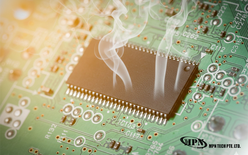
3. Thermal Management Problems
As the focus is typically placed on a PCB’s functionality and signal performance, thermal issues are often overlooked in early prototypes. However, they often become apparent quickly during testing.
In low-quantity or proof-of-concept designs, heat buildup may not be immediately apparent until extended testing begins. When heat dissipation is insufficient due to poor component spacing, lack of thermal vias, or limited thermal paths, localised overheating could occur. This is likely to affect component reliability and stability,
How to avoid it:
- Include thermal vias under heat-generating components
- Allow sufficient spacing between high-power parts
- Use copper pours or dedicated heat sinks where appropriate
4. Component Placement Errors
Incorrect component placement is a common PCB issue in early-stage designs, especially when boards are revised frequently. As components are added, removed, or repositioned across design iterations, it triggers errors such as incorrect orientation, insufficient spacing, or unclear reference markings.
These placement issues may result in assembly mistakes, poor soldering quality, or components not functioning as intended once the board is powered on. For one-off boards, a placement error often means starting from scratch or seeking specialised PCB repair services to salvage the board.
How to avoid it:
- Clearly mark polarity, pin-1 indicators, and reference designators
- Follow established design rules for spacing and orientation
- Review component placement with both electrical and assembly considerations in mind
5. Electromagnetic Interference (EMI)
Electromagnetic interference (EMI) issues possibly affect both circuit performance and measurement accuracy. When PCB layouts are poorly organised, grounding is inadequate, or shielding is insufficient, unwanted electromagnetic noise may couple into sensitive signal paths.
As this noise alters signal voltage levels or timing, it becomes harder to distinguish true signals from interference. This can reduce measurement accuracy, increase background noise, and cause the circuit to behave unpredictably during testing and analysis.
How to avoid it:
- Group related components to reduce loop areas
- Use proper grounding and decoupling techniques
- Route noisy and sensitive signals separately
How to Manage PCB Issues in Low-Quantity Prototyping
Common PCB problems are especially impactful in low-volume academic prototyping. For researchers working on single-unit or low-quantity boards, prevention is far more efficient than correction. However, when issues arise, access to a reliable provider of PCB repair in Singapore becomes important.
At MPN Tech, we support PCB projects by applying practical engineering expertise and performance-focused layout practices. We also help recover functional prototypes when issues arise, reducing the need to restart fabrication. With the right design and support, a well-engineered PCB enables efficient development and meaningful progress.
Contact us to explore our offerings.
 MPN Tech