
Key Takeaways:
What are Some Non-Destructive Testing Methods for PCB Production?
- X-ray inspection reveals internal features such as hidden solder joints and layer alignment issues, while also supporting root cause analysis by tracing defects back to their origin.
- Automated Optical Inspection focuses on visible accuracy, enabling early detection of placement and soldering errors so corrections can be made before failures occur.
- Ultrasonic testing verifies material integrity, making it especially valuable for boards exposed to repeated testing, thermal stress, or rework.
- Visual inspection remains a foundational step, providing fast feedback on surface quality even though it cannot detect internal defects.
Introduction
In modern electronics manufacturing, quality is defined as much by what cannot be seen as by what can. As circuit boards become more compact, multilayered, and functionally dense, ensuring reliability requires more than surface-level checks. When it comes to PCB production, quality control processes are designed to verify that every layer, joint, and connection performs as intended, even when defects are hidden from view.
This is where non-destructive testing methods play a critical role. Techniques such as X-ray inspection allow manufacturers to examine the internal structure of a PCB without damaging it. When combined with complementary inspection methods, these approaches form the foundation of a quality control process that supports both prototyping and full-scale electronics production later.
In this article, we examine the key inspection methods used in PCB quality control. Read on to understand the role each process plays at different stages of production.
Why Non-Destructive Testing Matters in PCB Quality Control
Non-destructive testing, commonly referred to as NDT, allows manufacturers to detect defects without altering or damaging the PCB itself. This is essential for complex assemblies where internal structures cannot be assessed visually. By identifying issues early, NDT reduces rework, prevents latent failures, and supports consistent performance across batches.
What are the Common NDT Techniques Used in PCB Production?
1. X-ray Inspection
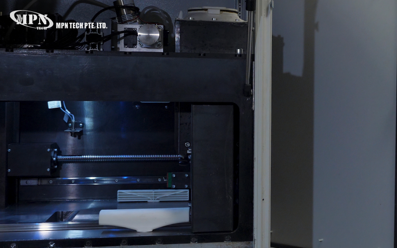
X-ray inspection is one of the most widely used NDT techniques in PCB manufacturing. By penetrating the board, X-ray systems reveal internal features that are otherwise inaccessible. This method is commonly applied to multilayer PCBs and assemblies where solder joints are not visible, such as those using ball grid arrays.
X-ray inspection also supports root cause analysis. Root cause analysis is a structured approach used to identify the underlying reason a defect or failure occurs. In the context of PCB fabrication in Singapore, this means examining where and how an issue first developed, such as during design, fabrication, or assembly. When failures occur, manufacturers can trace issues back to specific layers or processes rather than relying on surface-level assumptions.
2. Automated Optical Inspection
Automated Optical Inspection (AOI) focuses on the visible aspects of a PCB. This method is particularly effective for catching early-stage errors such as missing components or solder bridges.
High-resolution cameras detect deviations in component placement, orientation, and solder patterns with greater consistency than manual inspection. The system then compares captured images against reference data to identify defects that could affect performance. By addressing issues immediately after assembly, manufacturers can apply targeted corrections and reduce the risk of later failures or costly rework.
3. Ultrasonic Testing
Ultrasonic testing uses sound waves to detect internal fractures, delamination, or voids within the PCB substrate. While less commonly discussed than X-ray inspection, it plays an important role when material integrity is critical. In applications exposed to thermal cycling or mechanical stress, ultrasonic testing helps identify weaknesses that may not cause immediate failure but could degrade performance over time.
In research environments, boards are frequently handled, reworked, and modified. This increases the risk of hidden structural or assembly issues over time. Consistent inspection helps ensure that these changes do not compromise performance. At the same time, when PCB production scales, systematic inspection methods provide confidence that assembly quality remains consistent across all boards, not just a small sample.
4. Visual Inspection
Visual inspection remains a fundamental part of PCB quality control. Whether performed manually or with automated assistance, it focuses on surface defects, solder joint appearance, and overall workmanship. However, it cannot detect internal issues as it is limited to what can be seen on the surface of the PCB.
Components, solder joints, and traces that are buried within inner layers or beneath packages are not visible to the naked eye or standard imaging tools. As a result, defects such as internal cracks, layer misalignment, or hidden solder voids require other inspection methods that can examine the board’s internal structure. Although it cannot detect internal issues, visual inspection still provides immediate feedback and often serves as the first line of defence before more advanced methods are applied. For PCB design projects in Singapore, this step helps ensure that design intent is reflected accurately on the physical board.
What are the Benefits and Practical Considerations of NDT?
The primary advantage of NDT lies in early defect detection. Identifying issues before boards are integrated into systems helps reduce downstream failures and supports smoother production cycles. These methods also improve traceability, allowing manufacturers to refine fabrication and assembly processes based on inspection data.
However, advanced inspection techniques require specialised equipment and expertise, which can increase time and cost for low-volume projects. As a result, inspection depth is often calibrated to project requirements rather than applied uniformly.
Effective PCB quality control is therefore not about using the most advanced tools available, but about applying the right inspection methods at the appropriate stages. By combining X-ray inspection, AOI, ultrasonic testing, and visual checks, manufacturers establish a layered approach that addresses both visible and hidden risks while maintaining efficiency.
As a reliable PCB supplier in Singapore, MPN Tech supports PCB projects with practical engineering expertise, performance-focused layout decisions, and strict inspection practices. that ensure assembly accuracy is consistently monitored at scale.
Contact us and let us support your PCB production and prototyping processes.
 MPN Tech