
Key Takeaways:
What Affects PCB and IC Chipset Compatibility?
- The compatibility is affected by how well the physical layout, electrical behaviour, and thermal performance are aligned from the outset
- Footprint accuracy and correct pinout matching influence whether components assemble cleanly and function as intended.
- Signal integrity in PCB design affects data reliability and the repeatability of experimental results.
- Power stability and PCB thermal management play a key role in maintaining consistent chipset performance during extended testing.
- Prototyping and validation reveal compatibility limits early, particularly when small-batch research boards differ from production-scale builds.
Introduction
When designing electronic systems for research or prototyping, the relationship between the Printed Circuit Board (PCB) and the integrated circuit (IC) chipset plays a decisive role in whether a design performs as intended. Even well-planned schematics can encounter issues if physical layout, electrical behaviour, or operating conditions fail to meet the requirements.
Understanding how PCB design choices interact with integrated circuit chipset requirements helps bridge the gap between theoretical design and real-world performance. From footprint accuracy to routing discipline and power delivery, compatibility considerations influence both functionality and the reliability of data collected during research.
In this article, we examine how PCB and IC component compatibility influences design accuracy, testing reliability, and overall system performance.
Why PCB and IC Chipset Compatibility Matters
This compatibility is not limited to whether components can be physically mounted. It involves electrical, mechanical, and thermal alignment across the entire design lifecycle. In academic and research settings, boards are often built in small batches or revised frequently. This means early compatibility awareness is essential in reducing iteration cost and preserving experimental timelines.
What Determines the Compatibility
1. Footprint and Pinout Matching
The physical interface between the PCB and the IC chipset begins with correct footprint selection and pinout mapping. Each integrated circuit package defines pad geometry, pitch, and orientation that must be reflected precisely in the PCB layout. Errors at this stage can lead to misaligned solder joints, open connections, or unintended shorts that are difficult to diagnose after assembly.
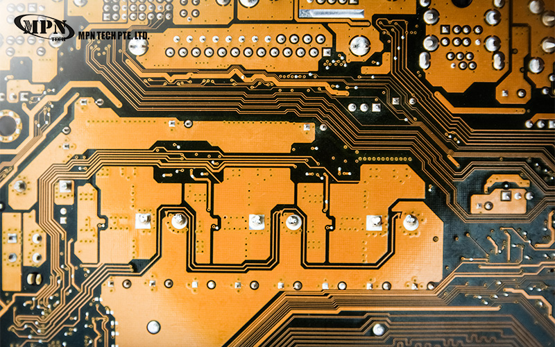
2. Signal Integrity and Routing Discipline
Signal integrity in PCB design becomes increasingly important as frequencies rise or analogue precision is required. Trace impedance, routing length, grounding strategy, and layer stack-up all influence how signals behave once they leave the chipset pins. Inadequate routing can introduce noise, reflections, or timing skew that alter experimental outcomes. To address these, working with an experienced PCB board manufacturer in Singapore helps preserve the accurate design intent through fabrication.
3. Voltage, Power, and Distribution Planning
Every chipset operates within defined voltage and current ranges that the PCB must support consistently. Power delivery networks that are underdesigned or poorly decoupled can cause intermittent faults that mimic logic errors or software instability. Stable power routing, appropriate bypass capacitors, and sensible plane allocation help ensure the chipset operates within specification during testing. This aspect is vital in research boards that interface with sensors or mixed-signal components.
4. Thermal Behaviour and Long-Term Reliability
Heat generation is an unavoidable aspect of integrated circuit operation, making PCB thermal management a critical design consideration. PCB layouts that ignore thermal paths risk performance drift or component degradation over time. Even in laboratory environments, sustained testing sessions can expose weaknesses in thermal planning. Copper pours, thermal vias, and airflow considerations allow heat to dissipate effectively without introducing mechanical stress. Thermal awareness supports both device longevity and experimental consistency when working with a chipset under continuous load.
5. Prototyping, Simulation, and Compatibility Testing
Simulation tools allow researchers to anticipate potential compatibility issues before fabrication, yet physical prototyping remains essential. Testing the PCB and chipset together under realistic operating conditions reveals interactions that simulations may not capture. A smooth PCB fabrication process in Singapore supports faster turnaround during this validation phase.
A practical limitation to acknowledge is that small-batch prototyping may not replicate mass-production tolerances. Results obtained from research boards should therefore be interpreted with awareness of fabrication scale and material variation.
How the Compatibility Improves Experimental Reliability
Understanding compatibility between the PCB and IC chipset allows researchers to translate theory into reliable hardware with fewer setbacks. From footprint accuracy to signal behaviour and thermal stability, informed design choices support credible experimental outcomes.
At MPN Tech, we support PCB projects with practical engineering expertise and performance-focused layout decisions. Our PCB manufacturing capabilities in Singapore keep subsequent prototypes electrically and mechanically consistent. This allows users to focus on analysis and experimentation rather than fault tracing.
Contact us to learn more about our offerings.

 MPN Tech