
Key Takeaways:
What Do CTE Values and CTE Mismatch Mean?
- These values quantify how PCB materials expand or contract with temperature changes and are measured in ppm/°C.
- Matching the values within practical tolerance ranges helps distribute stress more evenly across layers.
- CTE mismatch occurs when bonded materials expand at different rates, creating mechanical stress within the PCB structure.
Introduction
When designing printed circuit boards for prototyping, manufacturing, or research applications, material behaviour under heat is often overlooked. One material property that has a direct impact on long-term reliability is the Coefficient of Thermal Expansion, commonly referred to as CTE.
CTE describes how much a printed circuit board (PCB) and its constituent materials expand or contract as temperature changes. As every material has its own CTE value, differences in expansion behaviour can arise when multiple materials are bonded together within a PCB structure.
This article explains what the values mean in practical terms and why managing CTE mismatch is important in PCB design.
What Are CTE Values in PCB Materials?
The values describe how much a material expands or contracts when the temperature changes. Measured in parts per million per degree Celsius (ppm/°C), they indicate the dimensional change a material undergoes for each degree of temperature variation.
Why Matching CTE Values Matters
CTE considerations become more important as PCB designs in Singapore are exposed to higher temperatures, repeated thermal cycling, or increased structural complexity. Matching the values as closely as possible helps reduce thermal strain within a PCB structure. When bonded materials expand and contract at similar rates, mechanical stress is distributed more evenly across layers. This can lower the risk of deformation, cracking, or delamination over time.
However, this compatibility does not mean all materials must have identical values, which is rarely achievable in practice. Instead, designers aim for compatibility within acceptable tolerance ranges. These decisions influence laminate selection, stack-up design, and component choice, particularly for multilayer or high-temperature PCB applications.
When Does CTE Mismatch Occur and Why Should It Be Avoided?
CTE mismatch occurs when bonded materials within a PCB expand or contract at different rates as temperatures change. This is common because PCB assemblies combine materials with very different thermal behaviours. Standard FR-4 substrates have moderate CTE values that increase sharply once temperatures exceed their glass transition point. Copper layers, by contrast, expand at a lower and more stable rate. Ceramic components and chip packages expand far less than the surrounding laminate.
As these materials are physically bonded together, differences in expansion create stress at the interfaces between layers. This stress becomes more pronounced during repeated heating and cooling cycles, such as those experienced during soldering, reflow, or normal operation.
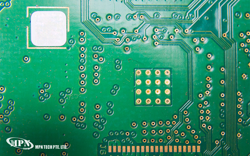
CTE mismatch should be avoided because differential expansion generates cyclic mechanical stress within the PCB structure. With repeated thermal cycling, this stress concentrates at material interfaces and plated through-holes, accelerating fatigue. Over time, this can lead to measurable failure modes such as warpage, interlayer delamination, cracked solder joints, and reduced reliability of vias and component terminations.
A Practical Limitation to Consider
It is worth noting that perfectly matching values across all materials is rarely achievable during PCB fabrication. Designers often need to balance thermal compatibility with other factors such as dielectric performance, availability, and cost. In some cases, controlled mismatch may be acceptable if mechanical stresses remain within proven limits.
For teams developing advanced PCB projects, working with experienced PCB board manufacturers in Singapore, such as MPN Tech, can help support more informed design and fabrication decisions. Our team possesses the technical know-how to reduce material-related risks across both prototyping and production stages.
Contact us to learn more about our expertise.
 MPN Tech